Application of Scanning Electron Microscope in Characterization of Metal Materials
Metal materials play an indispensable role in modern industry, and their performance directly affects product quality and service life. With the continuous development of materials science, higher requirements have been put forward for the microscopic structure and composition analysis of metal materials. As an advanced characterization tool, Scanning Electron Microscope (SEM) can provide high-resolution surface morphology information and combine with spectroscopic analysis techniques for elemental composition determination, making it an important tool in metal material research. This article aims to discuss the application of SEM technology in the characterization of metal materials and provide references and guidance for related research.
Basic Principles of Scanning Electron Microscope (SEM)
The working principle of a scanning electron microscope is based on the interaction between an electron beam and the sample surface. When a high-energy electron beam scans the sample surface, various signals are generated, including secondary electrons, backscattered electrons, characteristic X-rays, etc. These signals are collected by corresponding detectors and processed to form surface morphology images or elemental distribution maps of the sample.
SEM Sample Preparation for Metal Materials
Microstructural Analysis: CIQTEK EM provides high-resolution images to help researchers observe and analyze the microstructure of metals and composite materials, such as grain size, shape, phase distribution, and defects (e.g., cracks, and inclusions). This is crucial for understanding the relationship between material properties and processing techniques.
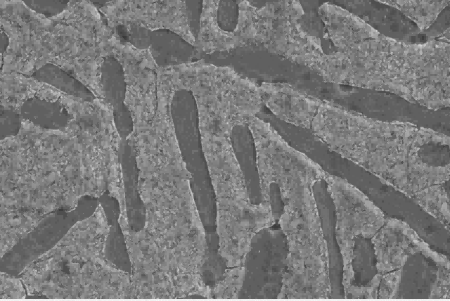
α + β Titanium Alloy
The heat-affected zone is the most vulnerable area in a welded joint. Studying the changes in the microstructure
and properties of the welded area are of great significance for solving welding issues and improving welding quality.
Composition Analysis: Equipped with an EDS or a WDS system, CIQTEK SEM allows for qualitative and quantitative elemental composition analysis. This is highly important for studying the distribution patterns of alloying elements and their impact on material properties.
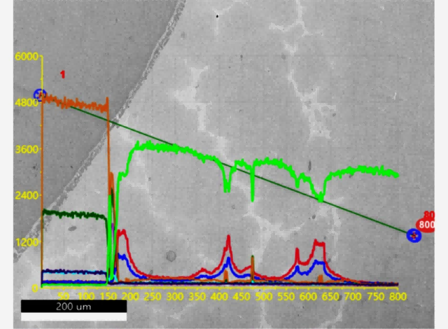
Elemental Line Analysis by EDS
By combining SEM with EDS analysis, the compositional changes and
element distribution of impurities in the welding area can be observed.
Failure Analysis: After failures such as fractures, corrosion, or other forms of damage occur in metals and composite materials, CIQTEK SEM is a key tool for analyzing mechanism failure. By examining fracture surfaces, corrosion products, etc., the root cause of the failure can be identified, providing insights for improving material reliability and lifespan.
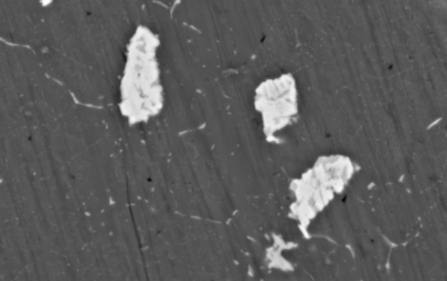
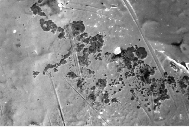
2A12 Failure of aluminum alloy components
2A12 aluminum alloy exhibits various precipitation phases, which can be distinguished morphologically as
large block-shaped, short rod-shaped, chain-like particles, and dispersed precipitates. The block-shaped phase
contains elements such as Al/Cu/Fe/Mn, while the other rod-shaped and chain-like precipitates are mainly
AI/Mg/Cu. Cracks propagate along the block-shaped hard phases.
New Material Development: In the process of developing new materials, CIQTEK SEM can be used to validate the synthesis of new materials and assess the structure and properties of nano-materials, multilayer films, nano-composites, and more. It drives advancements in materials science.
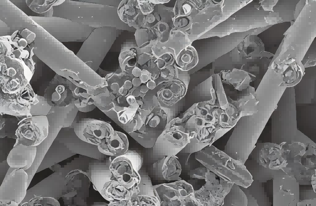
Ceramic
Silicon carbide ceramic substrate material is one of the preferred key thermal
structural materials for aerospace engine high-temperature components.
Interface Research: In composite materials, the characteristics of interfaces between different phases directly influence the overall performance of the composites. CIQTEK SEM can reveal detailed interface structures, assisting scientists in optimizing interfaces and enhancing the overall performance of composite materials.
Coating Analysis
A phenomenon of nickel coating detachment on the nickel-plated nut’s base material is observed, such failure causes oxidation
of the exposed substrate. After prolonged usage, the detachment area may become the failure point of the component.