How to eliminate vignetting/edge effects/charging effects
Creating a perfect image requires a combination of theoretical knowledge and practical experience and a balance between many factors. This process may encounter some challenging issues in the use of Electron Microscope.
- Astigmatism
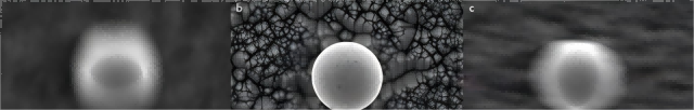
Astigmatism is one of the most difficult corrections to make in an image and requires practice. The middle image in the following figure is a correctly focused image after astigmatism correction. The left and right images are examples of poor astigmatism correction, resulting in stretched stripes in the image.
To achieve precise imaging, the cross-section of the Electron Beam (probe) should be circular when it reaches the specimen. The cross-section of the probe may become distorted, forming an elliptical shape. This can be caused by a series of factors such as machining accuracy and defects in the magnetic pole piece or copper winding in the casting of the ferromagnetic coil. This deformation is called vignetting and can result in difficulties in focusing.
Severe astigmatism is one of the most difficult corrections to make in an image and requires practice. The middle image in the following figure is a correctly focused image after astigmatism correction. The left and right images are examples of poor astigmatism correction, resulting in stretched stripes in the image. can manifest as “stripes” in the X direction in the image. As the image transitions from under-focus to over-focus, the stripes will change to the Y direction. When the focus is precise, the stripes disappear, and proper focusing can be achieved if the spot size is appropriate.
When magnified around 10,000 times, if there are no stripes in either direction when the objective is adjusted to under-focus or over-focus, it is generally considered that there is no astigmatism in the image. Astigmatism is usually negligible in images below 1000 times magnification.
The best approach to correct vignetting is to set the X and Y vignetter offsets to zero (i.e., no astigmatism correction) and then focus the specimen as finely as possible. Then adjust the X or Y astigmatism control (cannot be adjusted simultaneously) to obtain the best image and refocus.
- Edge Effects
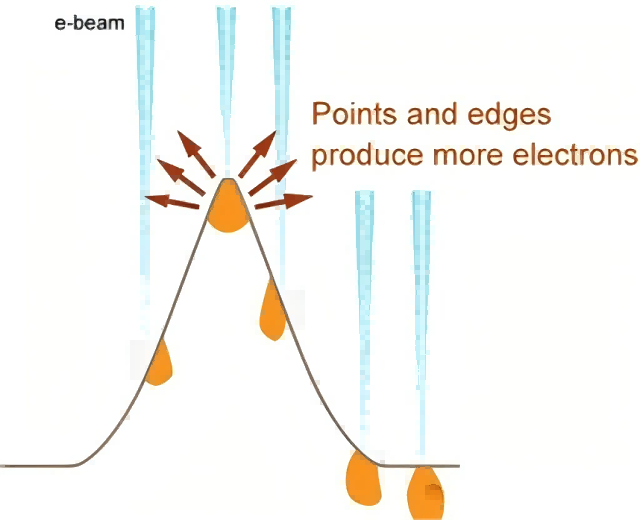
Edge effects occur due to enhanced Electron Emission at the edges of the specimen. The edge effects are caused by the influence of morphology on the generation of secondary electrons and are also the reason for the image contour produced by the secondary electron detector. Electrons preferentially flow towards the edges and peaks and emit from the edges and peaks, resulting in lower signal intensity in areas obstructed by the detector, such as recesses. Backscattered electrons emitted from the region of the sample facing the detector also enhance the topographic contrast. Reducing the accelerating voltage can reduce edge effects.
- Charging Effects
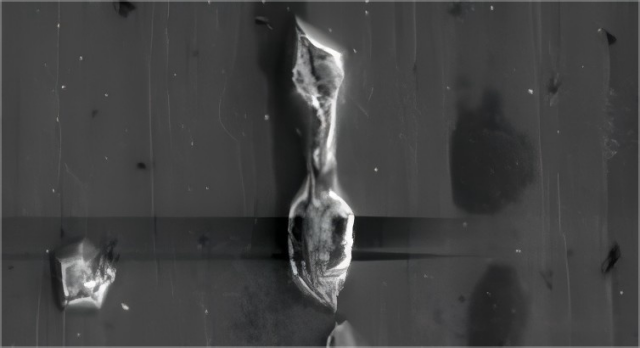
Uncontrolled discharge of electrons that accumulate in the sample can result in charging, producing unwanted artifacts, especially in secondary electron images. When the number of incident electrons is greater than the number of electrons emitted from the sample, negative charges can form at the locations where the electron beam strikes the sample. This phenomenon is called charging and can lead to a series of abnormal effects such as contrast anomalies, image distortion, and shift. Sometimes, sudden discharge of electrons from a charged region can cause bright flashes on the screen, making it impossible to capture uniformly contrasted sample images or even causing small samples to detach from the sample stage.
The severity of charging effects is related to (1) the energy of the electrons and (2) the number of electrons. The energy of electrons is related to the accelerating voltage, so reducing the accelerating voltage can reduce charging. The number of electrons is influenced by many parameters, including beam current, type of electron gun, spot size, and the aperture between the electron gun and the specimen. Therefore, adjusting these parameters can also help reduce the number of electrons and reduce charging effects.
To address charging issues in non-conductive samples, a common approach in sample preparation is to deposit a thicker layer of gold or platinum thin film on the sample. This is done to enhance the surface conductivity, allowing enough electrons to escape and avoiding surface charging and damage. Loose materials such as particles are often affected by charging. In practical operations, these samples are coated with a 3-10 nm thick metal layer using a sputter coater.