High-Resolution Scanning Electron Microscopy in Europe: Advancing Research and Industry
Scanning Electron Microscopy (SEM) has become an indispensable tool in various scientific and industrial fields, enabling researchers to explore the micro- and nanoscale world with unprecedented clarity. High-resolution SEM, in particular, has revolutionized materials science, life sciences, and semiconductor research, providing exceptional imaging capabilities and analytical precision. In Europe, where cutting-edge research and advanced manufacturing thrive, high-resolution SEM is a key driver of innovation.
The Growing Demand for High-Resolution SEM in Europe
Europe has long been at the forefront of scientific and technological advancements, with institutions and industries demanding ever-more precise imaging solutions. The rise of nanotechnology, semiconductor miniaturization, and biomaterial research has significantly increased the need for high-resolution SEM. Leading research centers, universities, and industrial R&D labs rely on these instruments to push the boundaries of discovery and product development.
Key Applications of High-Resolution SEM in Europe
- Materials Science – Researchers utilize high-resolution SEM to investigate the microstructure and composition of advanced materials, from novel alloys to nanocomposites. For instance, European automotive and aerospace industries rely on SEM to analyze lightweight composite materials, improving fuel efficiency and durability.
- Semiconductor Industry – As chip designs shrink to sub-10nm levels, European semiconductor manufacturers depend on high-resolution SEM for failure analysis, defect detection, and quality control. Companies in Germany and France use SEM to optimize lithography processes and ensure nanometer-scale precision.
- Life Sciences & Biotechnology – High-resolution SEM enables detailed imaging of biological samples, providing insights into cellular structures, biointerfaces, and medical device coatings. European pharmaceutical research facilities use SEM for drug delivery system studies and biomaterial innovations.
- Energy & Environmental Research – From battery technology to catalyst development, SEM plays a crucial role in optimizing materials for sustainable energy solutions. European renewable energy labs leverage SEM to enhance solar panel efficiency and improve hydrogen storage materials.
- Forensics & Cultural Heritage – Conservation scientists and forensic experts employ SEM for non-destructive analysis of historical artifacts and crime scene investigations. Museums in the UK and Italy use SEM to examine the composition of ancient paintings and sculptures, aiding in preservation efforts.
Choosing the Right High-Resolution SEM in Europe
Selecting the ideal high-resolution SEM depends on several factors, including resolution, electron source type, imaging modes, and ease of use. European laboratories and manufacturers prioritize instruments that combine superior imaging performance with user-friendly operation. Key considerations include:
- Resolution & Magnification – Resolving features at the nanometer or even sub-nanometer level is essential for high-precision applications. SEMs with resolutions below 1nm, such as those equipped with cold field emission guns (CFEG), offer superior clarity.
- Electron Source – Field Emission SEM (FE-SEM) offers the highest resolution and is widely used for advanced research. In Europe, many institutions prefer Schottky field emitters for their balance high brightness and operational stability.
- Analytical Capabilities – Energy Dispersive X-ray Spectroscopy (EDS) and Electron Backscatter Diffraction (EBSD) enhance the capabilities of SEM beyond imaging. European metallurgical research centers use these techniques to study grain structures and phase distributions.
- Automation & Workflow Efficiency – Modern SEM systems integrate AI-assisted imaging, automation, and remote operation to enhance productivity. In semiconductor fabs, automated defect detection algorithms reduce process variability and improve yield rates.
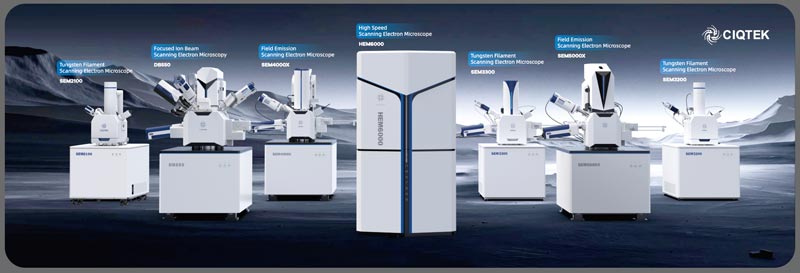
CIQTEK: Advancing High-Resolution SEM in Europe
CIQTEK is committed to providing high-performance scanning electron microscopy solutions tailored for European researchers and industries. Our cutting-edge SEM technology ensures exceptional resolution, robust analytical capabilities, and seamless usability for a wide range of applications.
In addition to technological superiority, CIQTEK stands out for its competitive pricing strategy. By offering high-resolution SEM systems at cost-effective prices, CIQTEK makes advanced electron microscopy accessible to a broader range of research institutions and industries without compromising on quality. This pricing advantage has been a key factor in its growing adoption across Europe.
Moreover, CIQTEK has established multiple electron microscopy bases and testing centers throughout Europe, including strategic locations in Germany, France, Italy, and the UK. These centers provide localized support, rapid service, and comprehensive training, ensuring that customers receive not only advanced equipment but also expert assistance to maximize their research outcomes.
Experience Next-Generation SEM Technology
Discover how CIQTEK’s high-resolution SEM can elevate your research and industry applications. Contact us today to learn more!